


Organic semiconductor materials constitute an important class of materials that have attracted much attention during the last years, especially in organic light emitting diodes (OLED). Organic field effect transistors (OFET) could replace their silicon-based counterparts in low-end applications with low production costs. However, the miniaturisation of these devices brings along the quest for nano-instruments that could elucidate the rich variety of physical processes, an understanding of which will be necessary to develop and to predict the function of new nanoscale devices.
The nano-instruments which are needed for this purpose could be simple nano-objects that are placed in the vicinity of the device under study. By measuring the perturbations exerted by the device on the nano-instrument, information could be obtained about the device’s working. In the past years the use of single molecules as sensitive nano-probes for processes in their local neighbourhood has been applied successfully. Therefore, we want to take the interaction of single molecules with electric fields and charge carriers as a good starting point for the study of the nanoscale electric processes. Ultimately we want to use single molecules as nano-instruments (e.g. voltmeter or amperemeter).
At low temperature the zero phonon lines of single molecules can be used as very sensitive probes for processes in the molecules’ neighbourhood, up to several nm away, as induced shifts of the order of 10-7 of the absolute optical frequency can easily be detected. Therefore we use single dye molecules as reporters for their local environment and we address the probes by means of optical single molecule microscopy and spectroscopy.
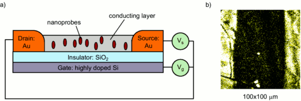
Figure 1: (a) Field effect transistor structure. (b) Confocal fluorescence image, 100 x 100 ?m2 of an anthracene crystal doped with dibenzoterrylene (DBT) molecules. The bright structures on the left and right of the image are the source and drain electrodes. The bright spots in the centre represent single DBT molecules.
The system we are working with consists of an organic FET, in which the conducting layer of an organic anthracene (Ac) crystal is doped with a very small concentration of dibenzoterrylene (DBT) dye molecules. In Figure 1a) you can see a schematic drawing of the FET, whereas in Figure 1b) you can see a confocal image of the real device. Here, the bright structures on the left and right of the image are the source and drain electrodes whereas the bright spots in the centre represent DBT molecules which are embedded in the Ac crystal.
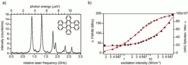
Figure 2: (a) Fluorescence excitation spectrum of dibenzoterrylene in an anthracene crystal at T = 1.4 K. The six narrow lines are the excitation lines of single dibenzoterrylene molecules. The inset shows the molecular structure of dibenzoterrylene. (b) Intensity dependence of the line width ??FWHM (circles) and the fluorescence count rate R (crosses) for a single dibenzoterrylene molecule in an anthracene crystal measured at T = 1.4 K. The red lines are the result of fits to the data points and yield ??FWHM(0) = 34 MHz, IS = 3 W/cm2 and Rinf = 100 000 cps.
In order to interpret the experimental results obtained from optical measurements on the probe molecules reacting to the applied fields in the FET structure, we first determined the photophysical properties of our host-guest-system. This includes things like the fully saturated emission rate Rinf, the unsaturated line width ??FWHM(0), the saturation intensity IS and photon bunching and anti-bunching experiments. Some of the results are depicted in Figure 2.
We furthermore determined the orientation of the DBT molecules in the Ac crystal, the vibronic fluorescence spectra and measured the Stark effect, i.e., their response to an applied electric field. The latter was accomplished by placing a crystal in a gap between two electrodes across which we applied an electric field. In this way we made sure that we did not inject charges from the electrodes into the crystal as is done in the FET structure. These measurements can be directly compared to the results of a molecular dynamics simulation of the insertion of DBT molecules in an Ac crystal. The MD simulations were carried out by P. Bordat and R. Brown from the University of Pau in France and agreed very well with our experimental data.
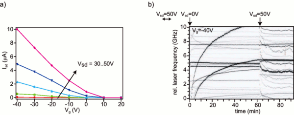
Figure 3: (a) Source-drain current versus gate voltage for different source-drain voltages of an Ac-crystal in a FET structure. The gate voltage commands the current for a given source-drain voltage, a characteristic signature of the field effect. Mobilities are up to ? = 2.8 x 10⁻⁴ cm/Vs for Vsd = 50 V. b) Stack of fluorescence-excitation spectra. At time t = 0 the source-drain voltage was switched from 50 V to 0 V. The spectral positions of the molecules (black lines) follow a nearly logarithmic law. At times t = 60 min, the source-drain voltage was changed again to 0 V. The gate voltage was at -40 V during the whole measurement.
The single-molecule characterisation gives us detailed insight in the properties of our host-guest system which we will need to interpret the data we obtain from our measurements on the nanoprobes in the OFET. In preliminary measurements we placed an Ac crystal doped with DBT on a field effect transistor as shown in Figure 1a). From the IV-characteristics in Figure 3a) it is clear that our Ac transistors correctly behaves as a FET at low temperatures. Figure 3b) shows the response of the absorption frequency of single DBT molecules (represented by the black lines) on an applied source-drain voltage.
The observed shifts show that our concept is working and that we can use single dye molecules as nano-instruments to study the charge transport in organic field effect transistors down to the nanoscale regime. We are currently investigating this in more detail.
References
- C. Hofmann, A. Nicolet, M.A. Kol´chenko, M. Orrit
“Towards nanoprobes for conduction in molecular crystals: dibenzoterrylene in anthracene crystals”
Chem. Phys. 318 (2005) 1-6